
Silicon Valley has long been the undisputed global capital of intangible value. It is the birthplace of the world’s most formidable software empires—Apple, Alphabet, and Meta—companies that have collectively generated trillions of dollars in market capitalization through code, design, and digital ecosystems. However, for decades, the physical landscape of the Valley has told a different story. While the software reached for the clouds, the architecture remained grounded in a monotonous sprawl of low-slung glass boxes and nondescript office parks. Most of the heavy lifting—the actual fabrication of the silicon that powers the modern world—migrated to massive "fabs" in Taiwan, South Korea, and the American Southwest.
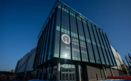
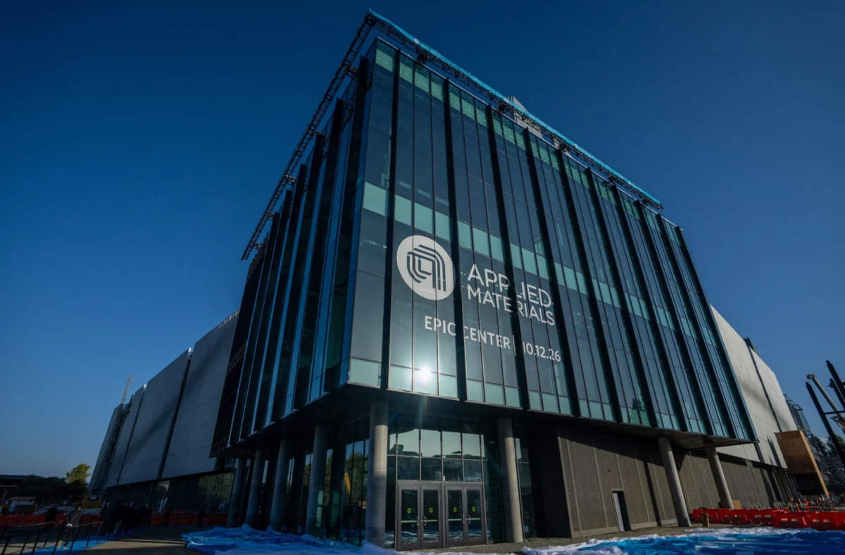
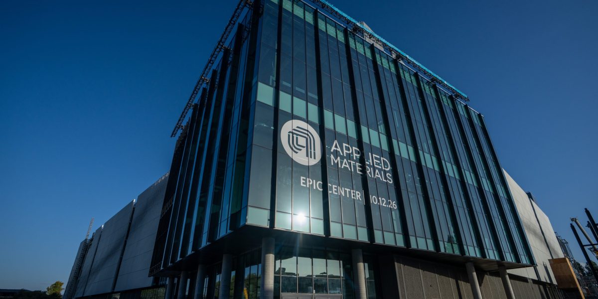
That narrative shifted dramatically this week. Applied Materials, the world’s largest producer of semiconductor manufacturing equipment, officially unveiled its Equipment and Process Innovation and Commercialization (EPIC) Center. Located on its Sunnyvale, California campus, the facility is a $5 billion statement of intent, signaling a return to "hard tech" dominance in the heart of the Santa Clara Valley.
Main Facts: A "Spaceship" for the Silicon Age
The EPIC Center is not merely an expansion of existing facilities; it is a monumental feat of industrial engineering designed to solve the most pressing bottleneck in the global economy: the speed of semiconductor innovation.
The statistics defining the facility are staggering. Spanning 600,000 square feet, the structure is a behemoth of glass, concrete, and steel. According to company officials, the facility utilized enough steel to construct two Eiffel Towers. Its most critical feature, however, is hidden within: a series of ultra-advanced "clean rooms" where researchers in protective "bunny suits" operate machines capable of etching microscopic circuits onto silicon wafers. These clean rooms alone occupy a space equivalent to three professional football fields.
The EPIC Center represents the largest-ever U.S. investment in advanced semiconductor equipment research and development (R&D). Rather than acting as a traditional manufacturing plant for commercial chips, EPIC is a collaborative laboratory. It is designed to host researchers from the world’s leading chipmakers—including Intel, TSMC, Samsung, Micron, and SK Hynix—under one roof. This "co-location" model allows these industry giants to work directly with Applied Materials’ engineers, gaining early access to the next generation of tools used to build microprocessors and memory chips.
The primary objective is speed. Currently, the journey of a new chip architecture from "concept to commercialization" typically takes 10 to 12 years. Applied Materials aims to slash that timeframe to as little as six years. In the hyper-competitive world of Artificial Intelligence (AI), where hardware requirements are evolving monthly, this acceleration is viewed as a strategic necessity.
Chronology: From Chemistry Supply to the AI Frontier
To understand the significance of the EPIC Center, one must look at the 59-year trajectory of Applied Materials. Founded in 1967, the company began as a modest chemistry supply firm serving the nascent semiconductor industry. As the "Silicon" in Silicon Valley became a reality, Applied Materials evolved into the primary architect of the machines that make chips possible.
For the past several decades, the industry followed a predictable rhythm defined by Moore’s Law. However, as transistors approached atomic scales, the physics of chipmaking became exponentially more difficult. Production migrated to Asia, where government subsidies and specialized labor pools created a "manufacturing gap" that left the United States dominant in design but reliant on overseas partners for physical production.
The construction of the EPIC Center began two years ago, catalyzed by the global realization that semiconductor leadership is a matter of national security. The project moved through its development phase as the AI boom—fueled by Large Language Models (LLMs)—created an insatiable demand for high-performance GPUs and high-bandwidth memory (HBM).
The unveiling on Monday serves as the culmination of this two-year sprint. It arrives at a moment when the U.S. government is aggressively pushing for "re-shoring" critical technology, and when Applied Materials is seeing its highest financial returns in history.
Supporting Data: The Economics of the Silicon Boom
The financial data surrounding Applied Materials underscores why the company is willing to bet $5 billion on a single R&D facility. The company has emerged as one of the primary beneficiaries of the AI revolution.
- Stock Performance: Over the past 12 months, Applied Materials’ shares have surged by more than 110%, reflecting investor confidence in the company’s role as the "arms dealer" of the AI race.
- Revenue Growth: In August, the company reported quarterly revenue of $9.12 billion, a 25% increase year-over-year.
- Future Visibility: CEO Gary Dickerson has stated that the company has visibility into customer demand reaching as far as 2030, an unusual degree of foresight in an industry traditionally plagued by "boom and bust" cycles.
However, the investment is not without risk. The semiconductor industry is notoriously cyclical. Critics and industry observers have noted that "visibility" is not the same as signed, non-cancelable contracts. If the current AI investment cycle cools, or if a global recession dampens demand for consumer electronics, the massive capital expenditure on facilities like EPIC could become a financial burden. Applied Materials is essentially betting $5 billion that the demand for more powerful, power-efficient chips is a permanent structural shift rather than a temporary bubble.
Official Responses: Winning the "AI Race"
The rhetoric from Applied Materials’ leadership during the unveiling was focused on global competitiveness and the unique nature of the current technological "inflection point."
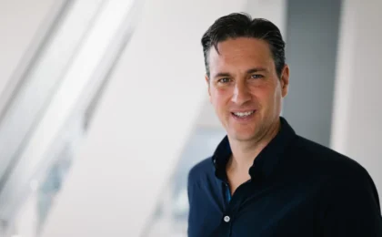
"Having innovators co-located together, having earlier access to the technologies that enable new AI architectures, is a complete game-changer," said Gary Dickerson, President and CEO of Applied Materials, in an interview with Fortune. He emphasized that the facility is designed to eliminate the "dead ends" that researchers often encounter when working in isolation. "Until companies collaborate in the lab, they don’t know what they don’t know," he added.
Dickerson’s comments also touched on the broader geopolitical landscape. He repeatedly invoked the necessity of "winning the AI race," though he remained measured regarding the complex relationship with China.
The stakes of this race were highlighted on the very day of the EPIC unveiling. CXMT, a prominent memory maker in China, announced a significant breakthrough in memory chip density. If verified, this advancement could allow CXMT to produce power-efficient memory chips that rival or surpass the current offerings from Samsung and SK Hynix. The news was immediate and jarring for the market; shares of Samsung and SK Hynix fell roughly 7% and 10%, respectively, in South Korea following the announcement.
Furthermore, Applied Materials continues to navigate a delicate regulatory environment. The U.S. Department of Commerce has placed strict export controls on advanced chipmaking equipment to China to prevent the country from developing the computing power necessary for advanced AI. In February, Applied Materials paid $252 million to settle a case with the Department of Commerce involving allegations of shipping equipment to China in violation of export restrictions.
Implications: A Strategic Weapon for National Security and Innovation
The EPIC Center represents more than just a corporate expansion; it carries significant implications for the future of Silicon Valley and the global balance of power.
1. The Re-Industrialization of Silicon Valley
For years, "innovation" in the Valley has been synonymous with software. The EPIC Center challenges this by proving that large-scale, high-tech industrial infrastructure can still thrive in California. While it is an R&D facility rather than a commercial high-volume manufacturing plant, it anchors the intellectual property of the "how" of chipmaking in the United States. It ensures that even if the chips are printed in Taiwan or Arizona, the machines and processes used to print them are perfected in Sunnyvale.
2. Collateral Collaboration
The "co-location" model is perhaps the most radical aspect of EPIC. By bringing fierce competitors like Micron and SK Hynix into the same building—albeit in private, secure test bays—Applied Materials is creating a hub-and-spoke model of innovation. This collective approach could prevent the fragmentation of standards and ensure that the entire industry moves toward AI-optimized architectures at a unified, faster pace.
3. Geopolitical Leverage
As China’s CXMT breakthrough demonstrates, the gap between Western and Chinese semiconductor capabilities is narrowing in certain sectors. The EPIC Center is the U.S. industry’s response to this narrowing gap. By cutting R&D cycles in half, the U.S. and its allies (TSMC, Samsung, SK Hynix) hope to maintain a "permanent lead" that China cannot bridge through traditional catch-up methods.
4. Environmental and Efficiency Pressures
A major focus of the EPIC Center will be power efficiency. AI models require massive amounts of energy, and the chips of the future must be significantly more efficient to make AI sustainable. The research conducted within EPIC’s clean rooms will likely focus on "Gate-All-Around" (GAA) transistor architectures and backside power delivery—technologies that are essential for the next generation of 2nm and 1.4nm chips.
In conclusion, Applied Materials’ $5 billion gamble is a testament to the belief that the AI revolution is the most significant technological shift of the 21st century. By building a "spaceship" in Sunnyvale, the company is not just creating a workspace; it is building a fortress designed to protect and accelerate the foundational technology of the modern age. As Gary Dickerson noted, "There’s never been an inflection like this in our lifetimes." The EPIC Center is now the ground zero for what happens next.